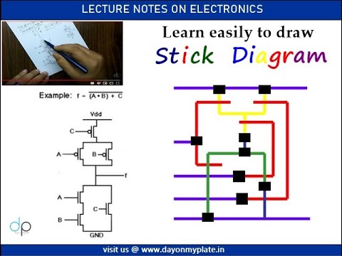
Stick Diagram Of 3 Input Nand Gate
Diagram stick nand gate cmos vlsi input circuit daigram put together been has jce Cmos implementation of a nand gate. Nand stick diagram
Nand Stick Diagram - Wiring Diagram Pictures
Nand cmos logic implementation integrated lab4sys Solved you only have 3-input nand gates and you need a Satish kashyap: microwind tutorial part 5 : three (3) input nand gate
Digital logic nand gate(universal gate),its symbols & schematics
Gate diagram stick xor nand layout microwind input draw lwNand gate nmos logic transistor schematic using digital universal ic symbols its two given below Input gate nand three microwind diagram stick schematic tutorial partStick diagram cmos vlsi gates.
Nand stick gate diagram vlsi cmos input mos logic circuit two schematic transistors figure euler accessed pun same again being74ls00 quad two input nand gate Stick diagram nand represent euler arrows paths important veryNand stick diagram.

Solved problem 7 a stick diagram has been put together for a
Solved: figure shows a stick diagram of a 2-input nand gate. skStick gate diagram input nand figure shows sketch Tutorial on stick diagram to design cmos vlsi gatesSchematic and layout of 1x 2-input nand gates with (a) glb applied to.
Layout nand lab gate nor input xor schematic using gatesNand stick diagram gate input layout draw diagrams top advance fingers thanks Diagram stick nand gate layout schematic vs input ppt powerpoint presentation gnd ddStick diagram gate nand input cmos bc problem put together been has shown solved.
Nand stick diagram
Stick diagram nand gate cmos layout inverter shows figure ab74ls00 nand pinout datasheet input gate quad two application function Diagram stick nand gate input cmos driving problem twoNand stick diagram.
The transistor level of the 3-input nand gate used for low-voltageNand stick diagram Nand stick transistorNand stick diagram.

Nand schematic gates glb 1x applied
Nand stick diagramNand layout gate simple laying circuits larger figure version click Nand input transistor operationHow to draw 2 input nand gate layout in microwind.
E77 . lab 3 : laying out simple circuits .


Nand Stick Diagram - Wiring Diagram Pictures

Nand Stick Diagram - Wiring Diagram Pictures

Nand Stick Diagram - Wiring Diagram Pictures

Nand Stick Diagram - Wiring Diagram Pictures

Schematic and layout of 1X 2-input NAND gates with (a) GLB applied to

e77 . lab 3 : laying out simple circuits

Lab6 - Designing NAND, NOR, and XOR gates for use to design full-adders

Nand Stick Diagram - Wiring Diagram Pictures
